From the magazine Phys.org. This is from a while ago—2013, in fact—but still really interesting.
Scientists use electron ‘ink’ to write on graphene ‘paper’
by Lisa Zyga, Phys.org

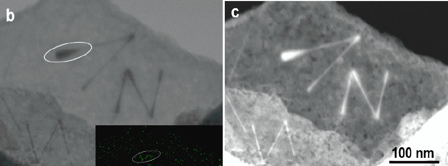
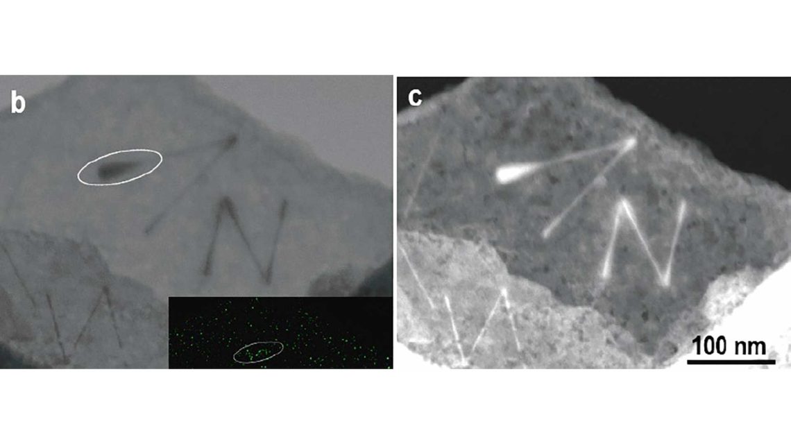
(Phys.org)—Nanoscale writing offers a reliable way to record information at extremely high densities, making it a promising tool for patterning nanostructures for a variety of electronic applications. In a recent study, scientists have demonstrated a simple yet effective way to write and draw on the nanoscale by using an electron beam to selectively break the carbon atoms in single-layer graphene.
The researchers, Wei Zhang and Luise Theil Kuhn at the Technical University of Denmark in Roskilde, Denmark; and Qiang Zhang and Meng-Qiang Zhao at Tsinghua University in Beijing, China, have published their study on using electron ink to write on graphene paper in a recent issue of Nanotechnology.
“The ability to record information has been directly correlated with the process of human civilization since ancient times,” Wei Zhang told Phys.org. “Paper and ink are the two essential factors to record history. Currently, information communication has proceeded onto an unprecedented scale.”
Nanoscale writing, which is essentially the manipulation of matter on the nanoscale, has already been widely explored. The current methods can be classified into two groups: lithography (top down), which imprints a pre-made pattern on a substrate, but has restricted resolution; and self-assembly (bottom up), which manipulates atoms or molecules individually, but faces challenges with controllability.
Herein, the researchers proposed a combination method based on both types of methods to overcome the difficulties of each, which they demonstrated on “the thinnest paper in the world”: graphene.
“The rise of graphene calls for broad attention,” Qiang Zhang said. “One distinct characteristic is its flatness, which provides the perfect opportunity to be regarded as the thinnest paper. In order to directly write on this ultimate thin paper, the suitable ink must be found. At the small scale, typically nanoscale, the ink candidate must meet the qualification as both high-resolution writing and visualization function. Therefore, high-energy electrons in a transmission electron microscope (TEM) are the best choice. The electron beam can be manipulated as ink for direct writing, but is by itself invisible.”

As the researchers explain, the carbon atoms in graphene are sensitive to a variety of irradiation effects. Here, a 300 keV electron beam was used to break local carbon-carbon bonds in single-layer graphene. When the bonds break, carbon atoms are kicked off, resulting in dangling bonds that are free to attract new carbon species from the vacuum and on the graphene surface. These new amorphous carbon species become absorbed onto the dangling bonds to stabilize the edge, forming only along the scanning direction of the electron beam.
“Our work demonstrates the feasibility of directly writing patterns on the thinnest material, graphene, in a position- and size-controllable style through manipulating electrons,” Wei Zhang said.
This technique offers both good controllability and high resolution. The researchers demonstrated a font size (defined by the width of the lines) as low as 2-3 nm. In addition, the graphene preserved its morphology after the writing process. With these advantages, the researchers hope that the new nanoscale writing technique will prove useful for future nanoscale writing and nanoelectronic applications, such as emerging microscale graphene circuits.
In the future, if further funding is available, the researchers hope to improve the resolution and efficiency of this nanoscale writing technique.
“More complex writing can be achieved by combining pre-defined shape design in the software,” Qiang Zhang said. “An ultimate goal is to achieve atomic scale writing easily and accurately for the design of electronic circuits.”
Explore further Writing graphene circuitry with ion ‘pens’
More information: Wei Zhang, et al. “Direct writing on graphene ‘paper’ by manipulating electrons as ‘invisible ink.'” Nanotechnology 24 (2013) 275301 (6pp). DOI: 10.1088/0957-4484/24/27/275301Journal information:Nanotechnology
© 2013 Phys.org. All rights reserved.
Here’s a more recent paper (September 17, 2021) about using silver particles on graphene oxide substrates: Synthesize [sic] and characterization of conductive nano silver/graphene oxide composites. It’s a scholarly paper from the the journal Science and Engineering of Composite Materials, so put on your science hat to read it! The full text is available at https://www.degruyter.com/document/doi/10.1515/secm-2021-0048/html.


